
UBM plasma activation prepares the surface so solder can spread and bond better on semiconductor pads. It cleans and activates the surface at a very small scale, improving wetting, bonding strength, and solder ball reliability. In semiconductor packaging, even tiny contamination can cause weak joints or defects. Plasma treatment removes these contaminants and increases surface energy, helping solder spread evenly and form stronger connections.
In this article, you will learn how plasma technology works, why wettability matters, and how it supports better bonding quality. We will also explain how UBM plasma activation helps reduce defects and improve process control using measurable data.
Understanding Plasma Activation at the UBM Level
Plasma is an ionized gas made of free electrons and active particles. When applied to a surface, it interacts at the molecular level. It modifies surfaces through cleaning, etching, and activation. These processes occur at a nano-scale level.
At the UBM interface, plasma removes thin oxide layers and organic contamination. At the same time, it introduces active functional groups that increase surface energy.
This transformation changes the surface from low-wetting to high-wetting behavior. It allows solder to spread more evenly during reflow.
Plasma Interaction with UBM Metal Layers
UBM layers typically consist of copper, nickel, and gold. These metals can form oxide layers during storage and processing.
Plasma treatment removes these oxides and activates the surface. It improves surface energy and prepares the interface for solder bonding.
This is especially important in flip chip packaging, where small pad sizes require precise wetting behavior.
Improving Wettability Through Surface Energy Control
Wettability describes how well a liquid spreads on a surface. In semiconductor packaging, this refers to how solder spreads on UBM.
A clean, high-energy surface allows better wetting improvement. Plasma treatment adhesion works by increasing this surface energy.
The relationship between surface condition and wettability can be summarized below.
| Surface Condition | Contact Angle | Wettability | Result |
| Contaminated Surface | High | Poor | Weak bonding |
| Plasma-Treated Surface | Low | Good | Strong bonding |
Plasma-treated surfaces show lower contact angles, which allows solder to spread more evenly and form stronger joints.
Lower contact angles indicate better wetting. Plasma reduces this angle by removing contaminants and activating the surface.
This directly improves bonding quality and reduces solder defects. Once surface energy is improved, the next impact appears in solder joint performance.
How Plasma Treatment Improves Solder Joint Performance
Clean and activated UBM surfaces allow solder to flow and bond correctly. This reduces voids and incomplete joints. Plasma treatment stabilizes solder spreading behavior and supports uniform joint formation.
Cold solder joints occur when solder does not fully melt or bond, often due to poor wetting. Plasma cleaning reduces this issue by preparing the surface before reflow. This improves yield and lowers the need for rework.
Activated surfaces also improve the chemical bonding between solder and UBM layers. This increases joint strength and helps the connection withstand stress. Stronger bonding supports better performance during temperature changes and mechanical loading.
Closed-Loop Process Control with Contact Angle Testing
Why Measurement Matters in Plasma Processing
Surface treatment should not rely on assumptions. It must be measurable and repeatable.
Contact angle testing is used to measure wettability. A lower contact angle means better wetting.
How Closed-Loop Systems Improve Yield
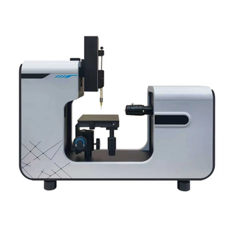
When plasma systems are combined with tools like the KeyLink Contact Angle Tester, they create a closed-loop system.
This means the surface is treated with plasma first. Then, its wettability is checked. If the result is not good enough, the process is adjusted.
This feedback loop ensures stable processing conditions. It helps reduce variation and improve production yield.
Comparing Plasma Treatment with Traditional Cleaning Methods
Traditional cleaning methods often rely on chemicals or solvents. These methods may leave residues or fail to remove ultra-thin contamination layers. Plasma offers a dry and precise alternative.
The differences between cleaning methods are shown in the comparison below.
| Method | Cleaning Level | Residue | Surface Activation |
| Chemical Cleaning | Moderate | Possible | Limited |
| Mechanical Cleaning | Low | None | None |
| Plasma Treatment | Nano-level | None | Strong |
Plasma treatment to improve adhesion provides both cleaning and activation in one step.
Types of Plasma Systems Used in Semiconductor Packaging
Atmospheric Plasma Systems
These systems operate in open air and are easy to integrate into production lines. They are suitable for inline processing.
Vacuum Plasma Systems
Vacuum systems provide uniform treatment across complex surfaces. They are ideal for precision applications like UBM preparation.

Automated Plasma Platforms
Modern systems use PLC control and programmable motion paths to maintain consistent treatment conditions. These features improve consistency and throughput.
Automated plasma systems can treat conductive and non-conductive materials while improving adhesion before bonding processes.
Why Plasma Technology is Essential for Advanced Packaging
As devices become smaller, surface precision becomes more critical. Plasma treatment supports fine-pitch soldering and advanced packaging designs by improving surface conditions. It also enhances process stability and yield. Stable surfaces reduce variation during assembly, which leads to fewer defects and more consistent results.
In addition, plasma is a dry process, so it reduces the need for chemicals and lowers waste generation.
Conclusion
Plasma treatment is no longer optional in semiconductor packaging. It plays a direct role in improving wettability, bonding quality, and solder ball reliability. With controlled process parameters such as power, gas flow, and exposure time, manufacturers can achieve repeatable surface activation
At KeyLink Technology, surface treatment solutions are designed to support real manufacturing needs. From nano-level cleaning to automated systems, these technologies help improve adhesion and overall process performance. If you are looking to improve bonding results, exploring our collection of plasma surface treatment systems is a practical next step.
Frequently Asked Questions
What is plasma treatment in semiconductor packaging?
It is a surface cleaning and activation process using ionized gas. It improves wettability and bonding before soldering.
How does plasma improve wettability?
It removes contamination and increases surface energy. This allows solder to spread more evenly.
Why is contact angle important?
It measures how well a liquid spreads on a surface. Lower angles indicate better wetting and bonding.


