
As a leading Plasma Surface Treatment systems manufacturer in Aste, we are committed to delivering innovative technologies and exceptional product quality to customers worldwide. Our plasma treatment solutions are designed to enhance surface cleaning, activation, adhesion, and coating performance across a wide range of industrial applications. We serve diverse industries including automotive, electronics, medical devices, printing, and packaging, providing reliable and efficient surface treatment systems. Wth acomprehensive portolo of standard equipment and customized solutions, we help manufacturers optimize production processes and achieve consistent, high-quality results.
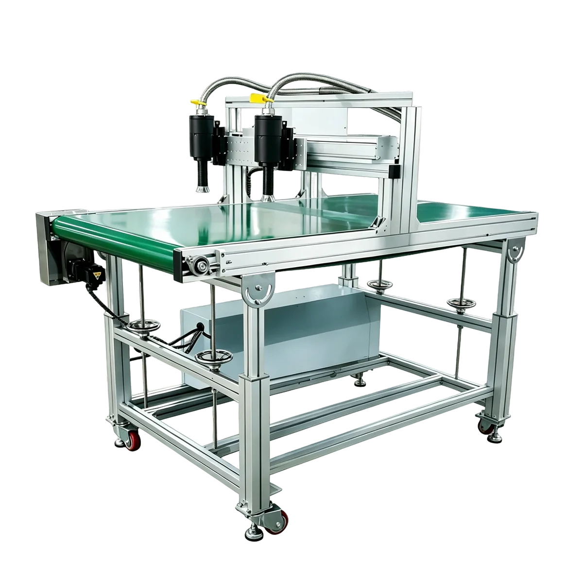
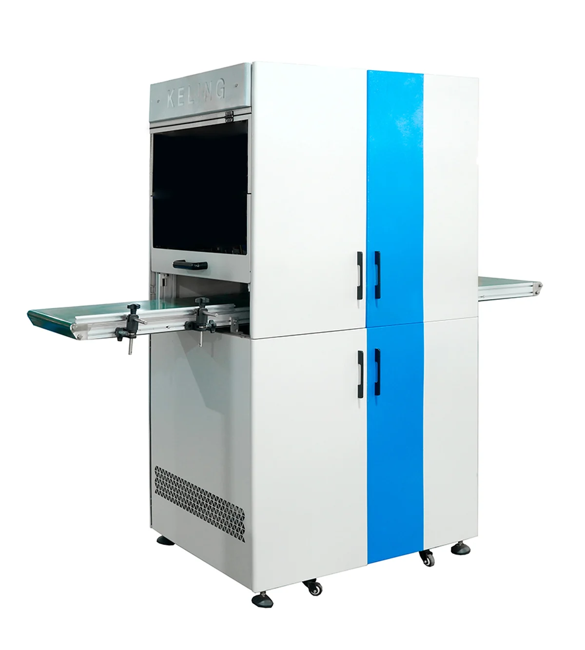
Our Plasma Surface Treatment Systems include both Amospheric end Vacuum Plasma technology, delivering high-performance surface activation, cleaning, end modifcation for a wide range of industrial applications. Designed for precise process control, user-friendly operation, and seamless integration into automated production lines, these
Systems help improve product quality, process consistency, and manufacturing efficiency.
KeyLink has focused on plasma surface treatment for over 15 years and is a leading manufacturer in China. We offer cost-effective integrated solutions and have supported top global brands like Apple, Valeo, Foxconn, and Bozhon with over 5,000 successful application cases.
We have three core strengths that enhance customer value: Free Sample Testing: Free sample testing with detailed plasma treatment evaluation reports
Advanced Testing Tools: Equipped with dyne pens, contact angle meters, and temperature sensors to meet various needs. Certified Products with Quality Guarantee: Certified with ISO9001, CE, LVD, and ETL, ensuring reliable quality.
We offer complete pre-sale and after-sale services, ensuring all global inquiries are responded to within 24 hours.


KeyLink Tech is a leading manufacturer of low-temperature plasma surface treatment machines, offering surface activation, cleaning, and adhesion enhancement. Backed by a 20-person R&D team, we provide advanced, customizable solutions. Certified by GB/T19001-2016, ISO 9001:2015, CE, and Intertek, ensuring high quality, safety, and innovation in every plasma system we deliver.

The trend in the packaging industry is adopting smart and sustainable solutions to make product packing more consumer-, brand-, and environmentally friendly. Smart packaging leverages technology will be more and more implemented such as QR codes, smart labels, RFID, and NFC chips
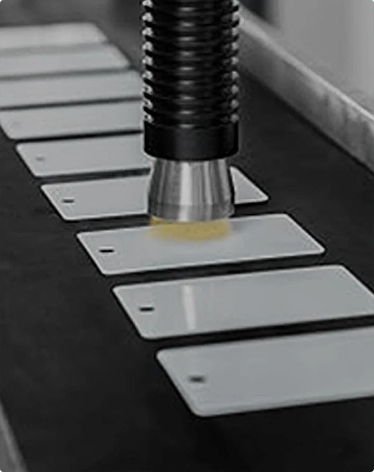
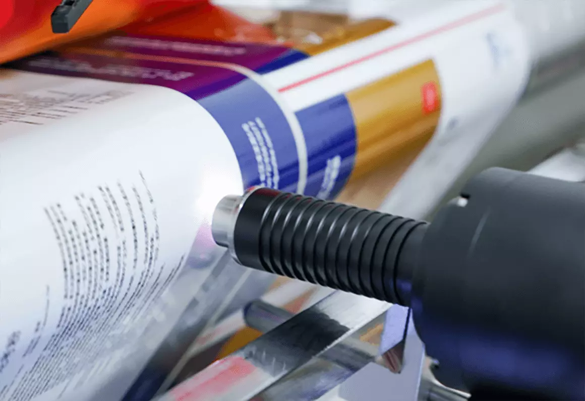
One of the key parameters determining the quality of the print is the adhesion of the ink to the substrate.

aterials with low surface energy such as PE, PVC, PP, PTFE, XLPE< EPDM, Silicone and other materials are difficult to be bonded with inks, sprayed or coated.

Nowadays modern customers have much higher expectations, such as reliable products, proactive service, personalized interactions, and connected experiences across digital channels.
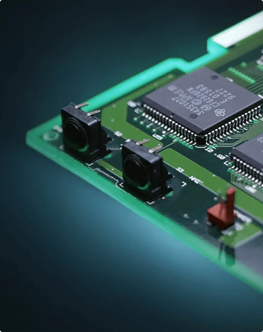
In the electronics industry, plasma pretreatment is a key asset for achieving cost-effectiveness and process reliability.

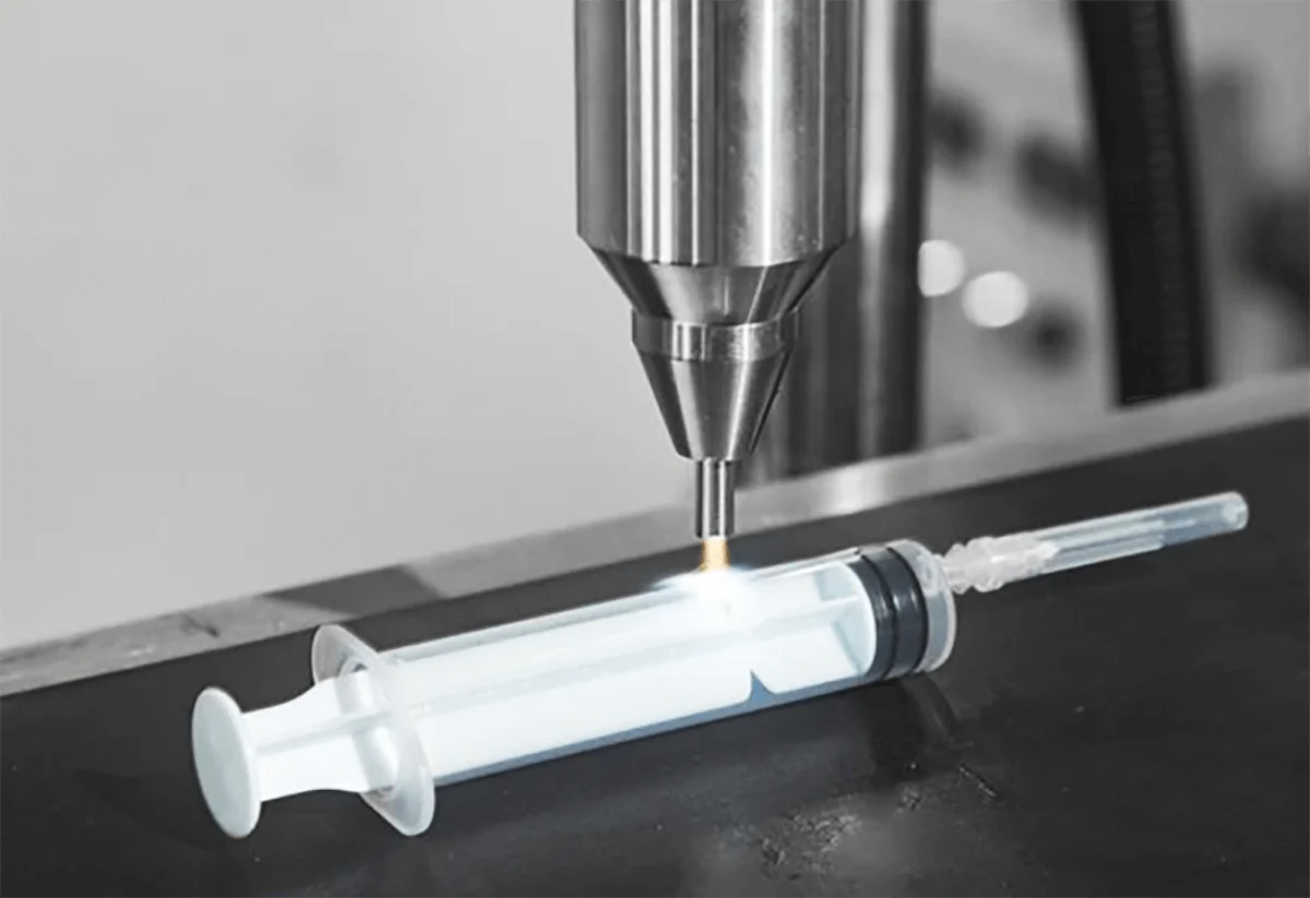
Plasma activation is the process of cleaning and activating a surface as a pre-treatment before applying an adhesive, coating or spraying.
Keylink Plasma Surface Treatment Systems improves its adhesion properties and is an optimal way to improve the strength of the chemical bond between the base material and the adhesive, coating or spraying. The application of the plasma activation process can significantly increase the cross-linking, reliability, and performance of a product.

Improving Bonding
Pre-treatment with Keylink Plasma Surface Treatment Systems increase the adhesion between an adhesive and a base material. It increases the peel and shear in the joint between the adhesive and the base material.

Plasma cleaning technology by using Keylink Plasma Surface Treatment Systems offers solutions for any type of contamination for any substrate. In the cleaning process microscopic contaminations will be removed from a surface by a dry method of turning the foreign particles into a gas. Nearly all materials can be treated. Plastics, metals, rubbers, ceramics or glass are suitable for plasma cleaning. It is an economical, safer, environmentally friendly and more efficient process in comparison to the traditional chemical cleaning method.

Using plasma technology for etching is an optimal treatment removing material from a polymer substrate, metal, oxide, glass or ceramic.There are various advantages to using plasma instead of traditional removal methods, such as chemical etching or mechanical abrasion.With plasma materials can be removed with high accuracy without any damage of the underlying substrate. Beside of this with plasma treatment very thin layers can be removed, the depth of material removal can be controlled precisely.
Copper alloys are widely used in electrical, electronic, automotive, and precision engineering applications where excellent conductivity, appearance, and surface quality are essential. During rolling, stamping, storage, and handling, the material surface often becomes contaminated with rolling oils, oxidation residues, organic
Customer Challenge PTFE (Polytetrafluoroethylene) is widely used in medical devices, electronics, and precision industrial applications due to its exceptional chemical resistance and low coefficient of friction. However, its extremely low surface energy makes it one of the most difficult polymers
WhatsApp us
Send us a message!
Our system experts are happy to assist you.