
Plasma-based pcb surface treatment removes contamination at the molecular level without touching solder pads or fine-pitch traces. Chemical etching and mechanical abrasion cannot make that claim.
This article compares the three approaches across cost, scrap rate, and environmental impact, and explains how in-line plasma systems fit into existing SMT and PCBA lines.
What Does Surface Preparation Mean For Bare PCBs?
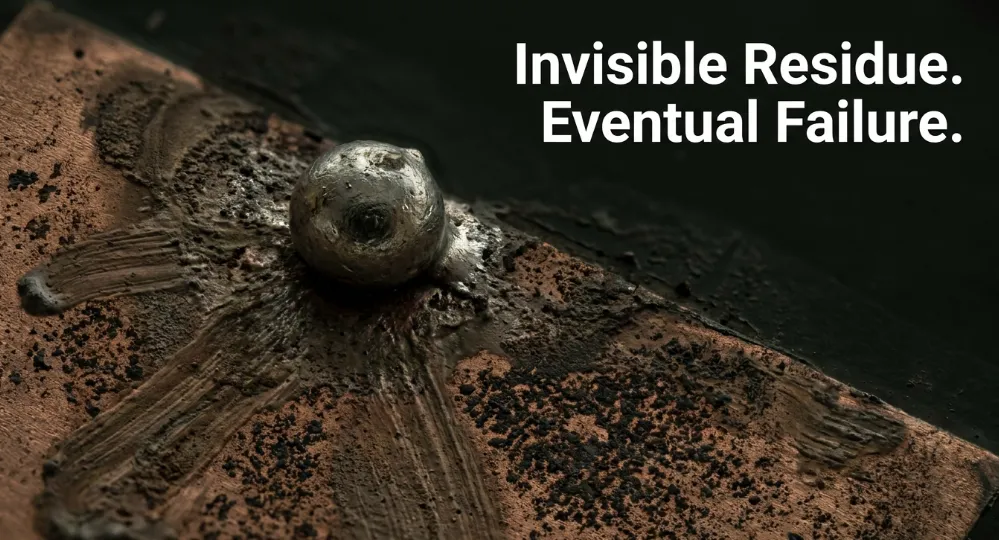
Every bare board carries invisible residue before assembly begins. Flux, oxidation, mold-release agents, and handling oils lower surface energy and block solder wetting. A proper pcb cleaning process removes these layers so solder joints form completely and coatings bond without voids underneath.
How Contamination Affects Solder Joints And Coatings
Low surface energy causes solder balls, dewetting, and thin spots in conformal coating. These defects often surface only after thermal cycling or humidity exposure once the product reaches the field, which makes them costly to trace back.
Which Standards Guide PCB Cleanliness Requirements?
IPC-A-610 and IPC J-STD-001 set acceptance criteria for solder joint quality and surface cleanliness across the electronics industry. Manufacturers use these standards to define pass or fail thresholds during incoming and in-process inspection.
How Does Plasma Compare To Traditional PCB Cleaning Methods?
A pcb washing process using solvents or aqueous chemistry dissolves surface residue, then requires rinsing and drying before the board moves forward. Rinse water must be treated before discharge, and some solvents fall under hazardous-waste rules in most regions.
Pcb plasma instead uses ionized gas to break contaminants into volatile byproducts removed by airflow or vacuum extraction. No liquid touches the board, so there is no drying step and no wastewater stream to manage afterward.
Chemical Etching And Mechanical Abrasion Limitations
Chemical etching can undercut fine copper traces if timing or concentration drifts even slightly. Mechanical abrasion risks scratching solder mask and dislodging small passive components on densely populated boards.
Environmental And ESG Considerations For Manufacturers
Replacing solvent-based cleaning with plasma removes a chemical waste stream from the process entirely. This directly supports ESG reporting goals tied to hazardous waste reduction and water use.
How Does In-Line Plasma Fit Into Existing SMT Lines?
In-line systems such as the PL-5010-IN mount directly into a conveyor between reflow and coating stations on the existing line. Treatment takes only seconds per panel, so overall throughput is not affected by the added step.
Positioning Plasma Before Conformal Coating Or Potting
Plasma pretreatment is a complementary step before conformal coating, not a replacement for HASL or ENIG finishing on the board. It prepares the surface for whichever coating or potting process follows next.
It also reduces solder defects earlier in the line by improving wetting before reflow, which lowers touch-up labor and rework costs downstream.
How Should Buyers Select Between Plasma And Traditional Cleaning?
Base the decision on board density, material sensitivity, and existing scrap data from the line. High-density boards with fine-pitch components benefit most from a dry, non-contact pcb surface treatment step.
Compare total cost of ownership rather than equipment price alone, including solvent purchase, wastewater treatment, and disposal fees against plasma’s electricity and compressed-air use.
What Does A Practical Selection Scenario Look Like?
A contract manufacturer producing automotive PCBAs was seeing coating delamination after routine humidity testing, traced to flux residue trapped under fine-pitch QFN packages that solvent cleaning had missed.
Switching to an in-line plasma step before coating raised surface energy consistently across the whole panel. Delamination complaints dropped after the change, and the line avoided adding a separate wet-cleaning station.
What Mistakes Should Buyers Avoid During Selection?
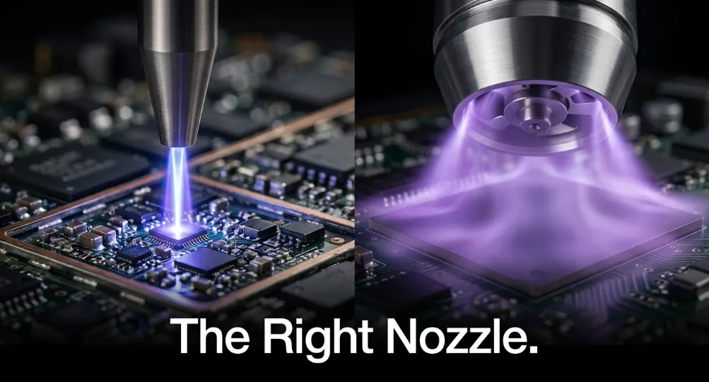
Do not assume one nozzle width suits every board layout. Narrow direct-jet nozzles work well for tight component spacing, while wider rotary nozzles suit more open panel layouts.
Skip sample testing at your own risk during evaluation. Request a treated sample panel with a surface-energy report before committing to any equipment purchase.
Conclusion
KeyLink Technology designs both direct-jet and in-line plasma systems for electronics manufacturers who need consistent surface preparation without chemical waste. Our guide on why plasma outperforms traditional PCB cleaning covers the mechanism in more depth for engineers evaluating a switch. KeyLink products carry ISO9001:2015 and CE certification, and our team supports vertically integrated solutions from core plasma generators to full line integration.
Explore our plasma surface treatment systems or contact our team to request a free sample test on your own boards.

PL-5010P Plasma Surface Treatment System
More DetailsFAQs
Does plasma treatment replace HASL or ENIG surface finishing?
No. Plasma is a pretreatment step that cleans and activates the board surface. It works alongside HASL or ENIG finishing rather than replacing either process.
Can plasma damage sensitive SMT components?
Properly configured plasma systems treat the surface without heat buildup or mechanical contact, so passives, connectors, and fine-pitch packages are not damaged during treatment.
How long does an in-line plasma cycle take per panel?
Most in-line systems treat a panel in a few seconds as it moves through the conveyor, matching typical SMT line speeds without adding delay.


