
Semiconductor cleaning removes contaminants to ensure wafers are defect-free. The goal is to remove organic residues, particles, and oxides without damaging the material. Both traditional chemicals and newer plasma technologies can clean wafers effectively.
What Makes Semiconductor Cleaning Critical?
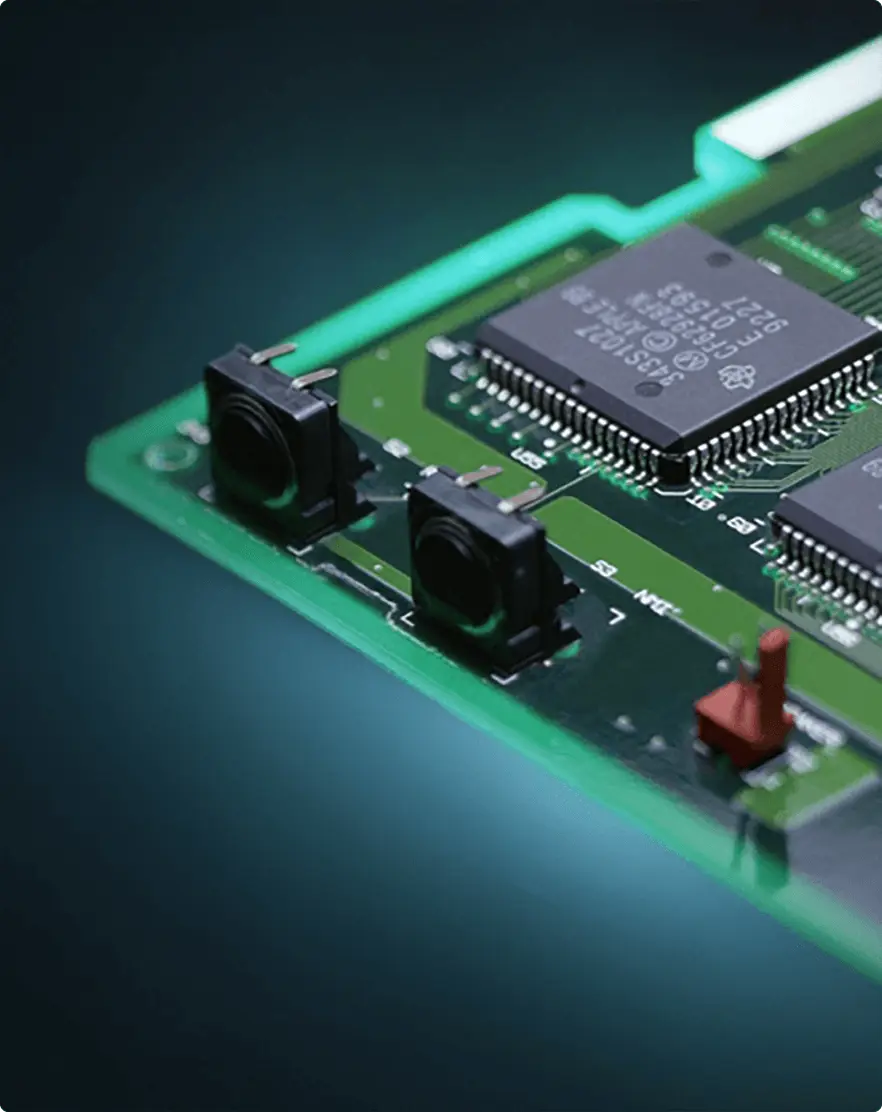
Contamination is a critical threat to semiconductor manufacturing. Dust, processing chemicals, and leftover residues all leave traces on wafers. If you don’t clean them timely, they can affect your device’s performance and reliability.
The consequences of inefficient cleaning can be severe. Your manufacturing yield may drop by 5–15% due to defects. Your products may fail because chips don’t work as intended. Even devices that ship can fail in the field, damaging your reputation.
Semiconductor decontamination removes organic residues, inorganic matter, and particles while preserving wafer integrity. That’s why cleaning is critical to manufacturing success.
What Are the Primary Contamination Challenges?
Modern semiconductor manufacturing faces three contamination challenges:
- Organic contaminants (photoresist residues, oils, grease) can trap moisture and interfere with bonding and coating.
- Inorganic deposits (metal oxides, minerals) can increase resistance and may degrade adhesion
- Particulate matter (dust, byproducts) can create micro-defects in circuits
These require rigorous semiconductor parts cleaning at nano-scales. Without effective removal of organic residues and particles, even tiny contaminants can compromise device performance.
What Steps Make Up The Traditional Semiconductor Cleaning Process?
The semiconductor cleaning process follows a structured six-step approach.

Step 1: Initial Cleaning
Water rinses remove loose particles first.
Then organic solvents like acetone dissolve oils, grease, and old photoresist. Organic solvent cleaning works well but creates hazardous waste.
Step 2: Oxide Removal
Oxide layers interfere with later steps, so they must be removed.
Hydrofluoric acid (HF) strips the oxide layer away, whereas Buffered oxide etch (BOE) solutions remove oxide more gently. Both methods work but create corrosive waste.
Step 3: Particle Removal
Particle removal must be done carefully. Aggressive cleaning can damage the wafer surface and render it unusable.
Semiconductor particle removal through sound waves (megasonics) creates tiny bubbles that pop and remove dirt without touching the wafer. Soft brushes also work for stubborn particles, but brush scrubbing can risk scratching delicate surfaces.
Step 4: Chemical Cleaning
Chemicals remove what’s left behind. The industry uses the RCA Clean method:
- RCA-1 uses hydrogen peroxide and ammonia to remove organic residues and particles
- RCA-2 uses hydrogen peroxide and hydrochloric acid to remove metal contamination
For heavy contamination, piranha clean uses sulfuric acid and hydrogen peroxide. Piranha clean works fast but is dangerous and creates hazardous waste.
Step 5: Final Rinse and Drying
The final stage removes leftover chemicals. Three methods handle this:
- Final rinse uses deionized water to wash away chemical residues
- Spin dryers use high-speed spinning and nitrogen gas to prevent moisture
- Marangoni drying uses IPA vapor to stop watermarks
Step 6: Quality Control
Quality control ensures cleaned wafers meet stringent standards.
- Optical microscopy and surface particle counters verify contaminant-free surfaces
- Surface roughness and particle count measurements confirm specifications are met
How Plasma Technologies Are Transforming Semiconductor Cleaning
Emerging plasma-based approaches offer significant advantages over traditional chemical methods. Plasma systems ionize gases to create high-energy particles that remove contaminants. This dry process eliminates organic residues and particles while activating surfaces without hazardous chemicals.
Plasma cleaning delivers several measurable benefits:
- Treats surfaces without damage or chemical residue
- Operators control every parameter for consistent results
- Costs a lot less than wet chemical methods
- Enables semiconductor packaging surface activation for improved bonding
KeyLink Technology offers vacuum plasma cleaners that treat up to eight wafer layers at once. Our atmospheric systems don’t require vacuum equipment and integrate easily into existing production lines. We also offer conveyor systems and automated equipment that process wafers at high volume without manual handling.
Real-World Results

Plasma technology has delivered measurable improvements across demanding manufacturing environments. KeyLink’s applications in semiconductor packaging, thin film processing, and material preparation demonstrate the technology’s effectiveness.
LED chip packaging: KeyLink plasma treatment before epoxy encapsulation increased adhesion strength by 40% while reducing void formation. Chips now survive thermal cycling in automotive and aerospace applications.
Thin film processing: On delicate thin film substrates, plasma cleaning removed organic residues without damaging the layers. Surface activation improved subsequent coating adhesion while preserving film integrity.
Aluminum substrate cleaning: Semiconductor surface modification through plasma treatment reduced contact angles from 65° to 28°, improving wettability and enabling 50% better adhesion for subsequent layers.
These results show that the technology is trusted in various high-reliability industries. KeyLink’s partnerships with national research institutions and manufacturers like Huawei, Foxconn, and BYD validate that plasma cleaning is reliable and effective for high-stakes applications.
Conclusion
Semiconductor cleaning is fundamental to manufacturing. Chemical methods work but generate waste and expense. Plasma-based semiconductor decontamination offers a better path forward.
With KeyLink’s plasma surface treatment technology, you eliminate hazardous chemicals and reduce costs. Plasma also activates surfaces for better adhesion without damaging materials. Plus, operators control every parameter for consistent results.
Whether you’ve just started or run established semiconductor packaging lines, plasma cleaning is key to device reliability and manufacturing success.


