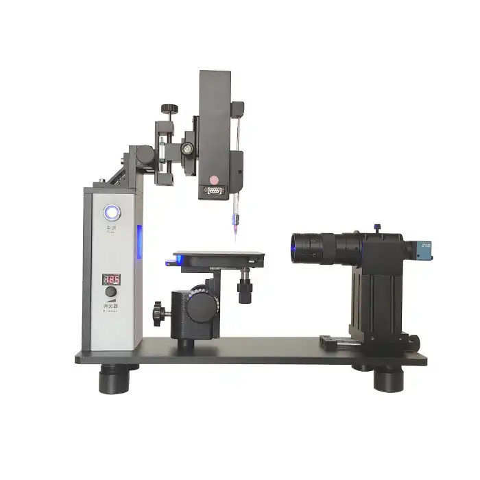
Contact angle meters, also known as tensiometers or goniometers, are widely used across various industries to measure the contact angle of a liquid on a solid surface, providing insights into wet-tability, surface energy, and adhesion properties. Key industries employing these instruments include materials science, coatings, pharmaceuticals, electronics, and automotive manufacturing.
Contact angle meters are often used to evaluate the effectiveness of plasma treatment by measuring the wettability of a surface after treatment. Plasma treatment modifies the surface properties of materials, and contact angle measurements provide a quantitative assessment of these changes, indicating the degree of hydrophilicity or hydrophobicity.
The basic principle of a contact angle meter involves placing a small droplet of the liquid onto the solid surface and then using a camera and analysis software to measure the angle formed by the droplet where it meets the surface. Optical tensiometers typically have a camera, a dispenser for creating the droplet, a sample stage, and a light source.
The contact angle (θ) is the angle formed between the liquid-solid interface and the liquid-vapor interface at the droplet’s edge. It indicates:
- Hydrophilicity (θ < 90°) – The surface is wettable (water spreads easily).
- Hydrophobicity (θ > 90°) – The surface repels water (droplets bead up).
Contact angle measurements are crucial in various scientific and industrial applications, including:
- Materials Science:
Contact angle measurements are crucial for characterizing the surface properties of new materials, predicting their behavior in applications, and optimizing material designs.
- Coatings and Paints:
The instruments are used to evaluate the quality and uniformity of coatings, ensuring proper adhesion and performance.
- Pharmaceuticals:
Contact angle measurements are vital for assessing the biocompatibility of medical devices and the wettability of drug coatings, impacting drug release and absorption.
- Electronics:
These measurements are used to control wettability on semiconductor chip surfaces, optimizing manufacturing processes and product performance.
- Automotive:
Contact angle measurements are used in the development of advanced materials, such as self-cleaning coatings and materials resistant to surface contamination.
- Aerospace:
Similar to the automotive industry, contact angle measurements are used to optimize materials for durability and reduce contamination.
- Printing and Packaging:
Contact angle measurements help in the evaluation of ink adhesion and the optimization of packaging materials for improved storage and printability.
- Surface Treatment:
Contact angle measurements are used to evaluate the effectiveness of surface treatments like plasma treatment, chemical etching, and flame treatment.
- Food Industry:
Contact angle measurements can help improve the printability and storage characteristics of food packaging materials.
Please contact Keylink Technology if you would like more details on specific Contact Angle Meters as well as Plasma Treatment Solutions designed to your applications!