
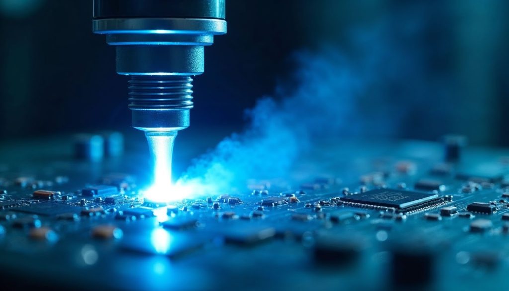
Potting and encapsulation protect sensitive electronics from moisture, vibration, and chemicals. However, without proper surface preparation, even the best materials can fail. Contamination, dust, and weak surface energy often lead to bubbles, delamination, and poor bonding. The fix? Plasma treatment for electronics.
In this guide, we explain why potting compounds fail, how plasma cleaning improves adhesion, and what benefits it brings to thermal, mechanical, and electrical reliability.
Why Potting Compounds Fail: Voids and Delamination Caused by Contamination

Potting and encapsulation are widely used to insulate, seal, and protect electronics. However, many failures can be traced back to one common problem: a dirty or inactive surface. When the surface isn’t properly prepared, trapped air and low surface energy prevent uniform wetting of the potting material.
The result? Voids between the encapsulant and substrate, poor adhesion, or even full delamination over time. These gaps can allow moisture ingress, reduce dielectric strength, and create localized overheating.
Common causes include:
- Flux residues or dust on the PCB
- Oxidation or weak boundary layers on plastic
- Improper handling or storage
These issues may not be visible but can sabotage the entire encapsulation process.
Using Plasma to Ensure a Perfectly Clean and Active Surface Before Potting

Plasma treatment for electronics solves this problem at the molecular level. Unlike traditional cleaning methods, plasma modifies the surface energy and removes invisible contaminants in one step.
Guarantees a void-free interface between the component and the encapsulant.
Plasma treatment for adhesion works by bombarding the surface with ionized gas. This process:
- Strips away organics, oxides, and dust
- Increases surface energy to promote wetting
- Enables better flow of epoxy, silicone, or polyurethane into small gaps
Especially for complex PCB assemblies or components with tight tolerances, plasma ensures that even the smallest corners are treated evenly. This helps reduce bubble formation and creates a uniform bond between the potting compound and the part, resulting in a stronger bond.
To further understand how plasma supports high-reliability bonding in critical components, take a look at this related guide on how plasma cleaning can solve semiconductor wire bonding failure.
The Result: Improved Thermal Management, Shock Resistance, and Long-Term Reliability
Electronics in demanding environments—such as EVs, aerospace, and industrial control systems—require more than protection. They need reliability over time. Proper plasma treatment before potting enhances:
- Thermal performance: Potting material stays in contact, improving heat dissipation
- Mechanical durability: Encapsulants cushion components better with no air gaps
- Electrical insulation: Cleaner, bubble-free encapsulation reduces arc risk
In long-term thermal cycling tests, soft potting compounds on plasma-treated surfaces show significantly fewer failures. Plasma treatment is especially beneficial for materials with low CTE mismatch tolerance.
Compatible with All Common Encapsulants
Plasma activation works across all resin types:
- Epoxy
- Polyurethane
- Silicone

It is also highly effective for sensitive substrates, such as plastics, glass, and ceramics. This versatility makes plasma treatment a go-to pre-treatment step for challenging applications, including potting LEDs, transformers, and high-voltage PCBs, where precision and reliability are non-negotiable.
To delve deeper into one of its most impactful applications, explore the benefits of plasma surface treatment in LED packaging.
Application Spotlight: PCB Plasma Treatment in Power Modules and Sensors
In PCB assembly, especially for power modules, sensors, and control units, plasma cleaning ensures stronger encapsulation bonding. These are often exposed to oil, heat, or vibration, and failure here can be costly.
PCB plasma treatment improves adhesion even on solder mask surfaces or populated components. Additionally, plasma removes oxidation from copper pads and protects them against chemical attack over time.
At KeyLink Technology, we’ve supported global brands with:
- Fully integrated inline plasma surface treatment systems
- Vacuum-compatible plasma chambers for sensitive electronics
- Custom robot systems for targeted cleaning
What to Look for in a Plasma System for Potting Applications
Choosing the right plasma treatment for electronics depends on your volume, part size, and substrate material. Here’s what matters most:
- Smart control interface: Enables recipe repeatability and production consistency
- Vacuum or atmospheric options: For deep cavity parts or open surfaces
- Multi-gas support: Some applications benefit from oxygen, argon, or CF-based gases
- Compact footprint: Important for integration in automated lines
KeyLink’s PL-6050P-S and PL-5050P series systems are trusted across various industries, including automotive, consumer electronics, and medical devices.
FAQ
What is plasma treatment for electronics?
Plasma treatment is a dry surface preparation method that cleans and activates electronic components, enhancing adhesion and reliability.
Why is plasma cleaning important before potting and encapsulation?
It removes invisible contamination, prevents bubbles, and ensures the potting compound bonds tightly without delamination.
Can plasma be used with any potting material?
Yes. Plasma treatment supports epoxy, polyurethane, silicone, and hybrid compounds.
Is plasma treatment safe for PCBs?
Absolutely. Plasma is a low-temperature and gentle process, making it ideal for sensitive electronics, including those with surface-mounted components.
How does it improve thermal management?
By eliminating voids and enhancing resin contact, plasma enables encapsulants to transfer heat more effectively.
Conclusion: A Clean Surface is the Foundation of a Reliable Encapsulation
No matter how advanced your potting compound is, it can only perform as well as the surface beneath it. Plasma treatment ensures that the surface is clean, activated, and ready to bond, solving common failure points before they begin.
At KeyLink Technology, we offer smart, scalable plasma systems built for electronic engineers who demand performance, reliability, and production speed. Whether you’re potting power electronics, sensors, or LED modules, we help ensure every bond counts. To learn how KeyLink Technology can help you integrate plasma treatment into your potting line, visit our solutions page.


