
Benefits of Plasma Treatment for Electronic Products
In electronics manufacturing, achieving precision, reliability, and sustainability is paramount. One method that addresses these needs effectively is plasma treatment.

Plasma treatment is a fast, eco-friendly process utilized primarily for two main purposes:
- Fine cleaning
- Surface modification
The innovative cleaning method is necessary in preparing surfaces for further processing. Plasma treatment offers a range of benefits. These include enhancing adhesion and improving the overall performance of electric components.
One primary advantage of plasma treatment is improving adhesion. Plasma treatment increases surface energy and reduces surface tension. These effects make materials more receptive to adhesives, coatings, and solders. The mentioned feature is crucial in producing printed circuit boards (PCBs).
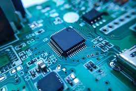
Plasma treatment provides an additional advantage known as the “micro-blasting” effect. This process is driven by ion bombardment. The micro-blasting effect removes contaminants and surface material at a microscopic level.
Plasma cleaning produces a clean, modified surface resulting in easy bonding and coating. This quality is valuable for delicate components. These are very delicate that even the slightest contamination can cause defects.
Plasma treatment also enhances the wettability of surfaces. By modifying surface properties, plasma treatment creates a more uniform coating application.
Application of Plasma Surface Treatment in Electronic Products
Plasma surface treatment is widely used in electronics manufacturing. It is effective for cleaning, surface activation, and etching. This cutting-edge cleaning treatment is helpful in industries such as the following:
- Telecommunications
- Automotive electronics
- Medical devices
For instance, plasma treatment is essential in preparing surfaces for coating and bonding.
For PCBs and other electronic assemblies, plasma treatment removes oils, silicones, and oxidation layers. These invisible contaminants can greatly impact electronic performance.
Plasma treatment breaks them down using UV radiation and ion bombardment. This process turns contaminants into volatile compounds that are easily removed. Thus, plasma treatment ensures strong bonds for coatings or adhesives.
Plasma surface treatment is also employed in fabricating microchips, sensors, and semiconductor wafers. In these applications, plasma surface treatment machines modify the surface at an atomic level.
The plasma process can be fine-tuned by adjusting the power level, treatment time, and gas type. This flexibility makes plasma treatment a versatile tool in electronics manufacturing. It also enhances efficiency across various applications.
Other Common Surface Treatment Methods in the Field of Electronic Manufacturing
Plasma treatment is indeed the preferred choice in electronics manufacturing. However, other methods are still available. Check them out below:
Chemical Cleaning
This method uses solvents or acids to remove contaminants. While effective, chemical cleaning often leaves residues. It also requires careful handling due to the toxic nature of the chemicals involved.
Laser Treatment
Laser technology is used for precise surface modification. However, it can be costly. Also, the heat generated during the process can pose a risk to heat-sensitive materials. The latter is common in electronics.
Mechanical Abrasion
This involves physically removing the top layer of material using sanding or grinding. Although effective, this approach can damage sensitive electronic components.
Summary
In conclusion, plasma treatment is a game-changer for electronics manufacturing. It offers superior benefits like improved adhesion, surface cleaning, and modification. These are necessary in producing quality electronic components.
Plasma surface treatment machines are also versatile. They handle a wide variety of materials and applications. This feature makes them indispensable for high-tech industries.
As a leader in this field, Keylink Technology provides innovative plasma systems. Their products are tailored to the specific needs of different businesses.
Delivering over 2,000 pre-treatment solutions annually, Keylink has achieved the following for its clientele:
- Increased efficiency
- Enhanced product quality
- Reduced environmental footprint


