Enabling Superior Performance & Production Reliability
As an expert in surface optimization for electronics manufacturing, KeyLink utilizes advanced plasma tech systems to deliver ultra-clean processing, enhanced adhesion, and extended product lifespan for PCBs, semiconductors, and components, helping you achieve cost-effectiveness and eco-friendly production.
The electronics industry relies on versatile materials like printed circuit boards for crucial hardware. Modern products demand miniaturization and reliability, but traditional joining can cause damage. Plasma surface treatment makes sensitive, low-wettability plastic parts receptive to bonding agents without harm. For manufacturers, plasma cleaning effectively removes invisible contaminants like organic residues, ensuring pristine surfaces and enhancing product reliability and lifespan. This technology is indispensable for functionality and long-term device reliability.

KeyLink plasma surface treatment systems are vital for optimizing processes in electronics manufacturing, providing effective surface preparation solutions for core components.
Plasma cleaning is widely used for cleaning printed circuit boards (PCBs), ensuring functionality and long-term reliability. It effectively removes organic contaminants and oxides from PCB surfaces, breaking down microscopic residues without harsh chemicals. This enhances solderability and boosts adhesion for coatings. Plasma penetrates tiny gaps, decreasing surface resistance. It’s crucial for preparing pcb surface finish for advanced packaging, making how to clean pcb before soldering a key step.

Prior to assembly, electronic components like semiconductor wafers, connectors, and various IC packages must be impeccably clean to ensure optimal electrical contact and adhesive bonds. Plasma cleaning removes organic contaminants, enhancing surface wettability and ensuring subsequent processes like wire bonding or epoxy application are more reliable. Before the wire bonding process, surfaces must be extremely clean to form a strong, reliable bond; plasma cleaning effectively removes any oxidation and contaminants that could interfere with this bonding, significantly improving bond integrity and device performance.
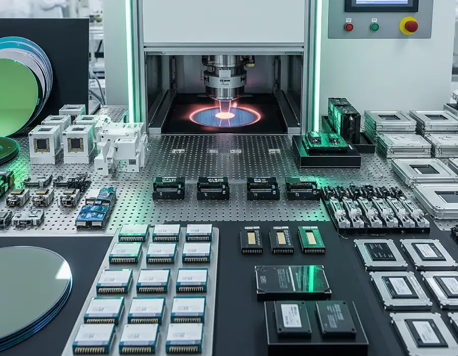
Using plasma cleaning before potting PCBA is essential. It cleanses the PCB surface by removing contaminants and creating micro-roughness, enhancing adhesion for potting materials. This prevents delamination and voids. Plasma treatment surface energy allows potting compounds to spread uniformly and penetrate gaps, reducing air pockets. This ensures optimal adhesion, reliability, and longevity of potted PCBAs.
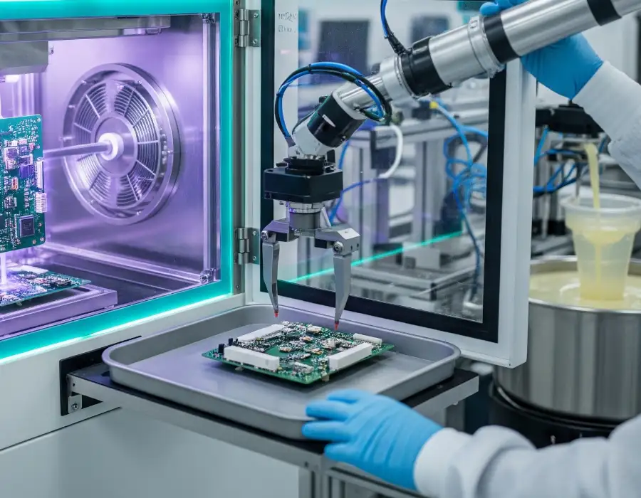
Before applying conformal coatings to electronic components for environmental protection, the surface must be free of contaminants that could interfere with adhesion. Plasma cleaning prepares the surface, making it more receptive to the conformal coating, which enhances its effectiveness and longevity. Electronic components are often sealed in packages to protect them from environmental factors like moisture, dust, and temperature variations. Organic contaminants on the surface can compromise this seal; plasma cleaning removes these, ensuring a more robust and long-lasting package seal.

Plasma technology is crucial for metal keyboard frames as an essential pretreatment before coating or painting. It effectively removes invisible contaminants like oils, oxides, and grease at a molecular level, leaving no chemical residues. This eliminates weak oxide layers, preventing corrosion. Plasma activation increases plasma treatment surface energy by introducing polar groups, making surfaces “paint-friendly” for uniform coating spread. This eco-friendly method replaces hazardous techniques, improving coating durability and performance.

Plasma pretreatment dramatically improves adhesion in LED devices by increasing surface energy and wettability. This is critical for bonding LED chips, applying conformal coatings, and layering organic materials in OLEDs. It enables better electrical contact, reduces thermal stress, and enhances mechanical stability and long-term reliability.
In OLED fabrication, plasma pretreatment simplifies processes via selective etching, offering cost and yield advantages. It also optimizes flexible OLED electrodes, improving optoelectronic performance and bending test results.
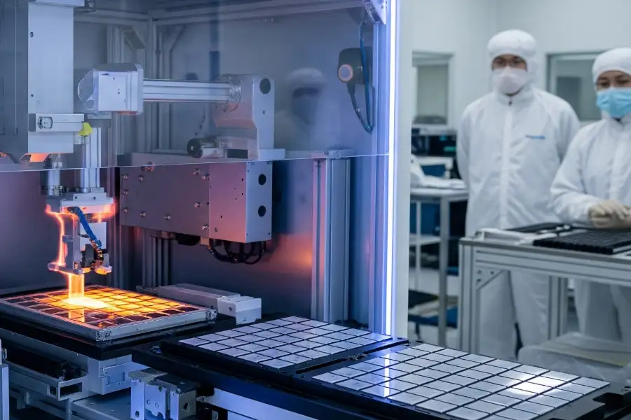
KeyLink offers a comprehensive range of plasma surface treatment systems to address diverse needs in electronics manufacturing, from precise localized treatment to high-throughput automated lines.
Our atmospheric plasma systems operate at ambient pressure, ideal for large PCBs and quick cleaning. They are designed for continuous processing and inline PCB manufacturing, mainly using chemical reactions to break down organic contaminants.
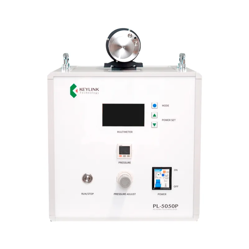
(Rotary Nozzle Type): Designed for complex surfaces and large-area treatment, such as lithium battery blue film bonding and electronics silk screen printing. Treatment width: 70-110mm.

(Automatic XYZ-Axis Platform): Features PLC + touchscreen control, with customizable X/Y/Z axis travel, suitable for 3C electronic accessories, like mobile phone screen pretreatment, phone case cleaning, and printing. Treatment width less than 100mm.

(Inline Plasma Treatment System) : Conveyor belt design, supports multi-gun configurations, with speeds of 0-30m/min, suitable for inline production in optoelectronics, plastics, consumer electronics, and printing.

(External Air Supply Jet Type): Improves adhesion for bonding and printing inks. The PL-5010P-OUT is a high-power model with continuously adjustable output, suitable for high-precision, complex, irregular materials like mobile phone screen dispensing. Max treatment width: 13mm.
Our low-temperature plasma systems operate under low-pressure or vacuum conditions, combining chemical and physical cleaning. They are more effective for stubborn residues and fine-pitch PCB cleaning due to higher ion energy. Ideal for precision cleaning and high-reliability PCBs, used in semiconductor and high-end PCB manufacturing.

(Vacuum Plasma Cleaning Machine) : Significantly improves microscopic treatment for materials like silicone, plastics, metals, glass, and polymers, including organic removal, inorganic cleaning, plasma surface activation, etching, and grafting. Customizable chamber capacity (10L-80L) and layers, offering high precision, fast response, large capacity, and precise control. Widely used in aerospace, precision electronic components, semiconductor packaging, automotive interiors, medical devices, and nano new materials industries.

(Vacuum Plasma Cleaning Machine) : Significantly improves microscopic treatment for materials like silicone, plastics, metals, glass, and polymers, including organic removal, inorganic cleaning, plasma surface activation, etching, and grafting. Customizable chamber capacity (10L-80L) and layers, offering high precision, fast response, large capacity, and precise control. Widely used in aerospace, precision electronic components, semiconductor packaging, automotive interiors, medical devices, and nano new materials industries.
Contact KeyLink: Begin Your Electronics Manufacturing Plasma Upgrade Journey
Optimize your electronics manufacturing with KeyLink’s advanced plasma surface treatment technology. Let our experts help you achieve superior performance, reliability, and efficiency.
Our Advantages in Electronics Manufacturing
KeyLink Technology offers state-of-the-art plasma treatment equipment designed to meet the rigorous demands of electronics manufacturing. Our systems are engineered for superior performance, integration, and environmental responsibility.
Our plasma solutions directly enhance electronics reliability. By optimizing bonding and effectively removing microscopic contaminants, we inherently extend component lifespan, leading to robust, durable products and reduced failure rates.
The plasma treatment process is compatible with nearly all electronic materials—plastics, polymers, glass, metals, and ceramics. This non-damaging method cleans and activates surfaces precisely, eliminating the need for varied, less effective chemical or mechanical treatments.
Plasma surface treatment is a dry, low-temperature process, requiring minimal energy and generating no harmful waste. It replaces hazardous chemical methods, significantly reducing disposal costs and contributing to substantial long-term operational savings.
Plasma cleaning offers rapid surface preparation, typically taking minutes, essential for high-throughput electronic manufacturing. Our plasma surface treatment systems integrate effortlessly into existing production lines, ensuring consistent results and increased output.
Choosing KeyLink Technology means partnering with an established leader dedicated to advancing industrial surface solutions. We are your ideal manufacturing partner, focused on delivering impactful results.

KeyLink Technology strategically operates in key Chinese manufacturing hubs (Zhejiang, Jiangsu, Guangdong), driving new energy advancements and serving lithium battery manufacturers. Our global network spans over 100 countries across Asia, Europe, Middle East, and North America, ensuring responsive support.
With over a decade of experience, KeyLink combines in-house R&D with strategic partnerships, holding ISO, CE, UL, and ETL certifications. We offer customized solutions and expert technical assistance, ensuring precise integration into your existing production lines.
Get an expert on the phone
Write us what we can do for you
You know exactly what you’re looking for
WhatsApp us
Send us a message!
Our system experts are happy to assist you.

